High Gradient Accelerator Sections
This work-package concerns the study, realization and characterization of electromagnetic linear accelerator X band sections for high gradients. The present technology of the S-band cavity allows to achieve accelerating electric fields of the order of 25 MV/m, while the C-band may reach 35 MV/m, and the X-band up to ~ 100 MV/m. To achieve electric fields 2-3 orders of magnitude higher, i.e. of the order of ~ 100 GV/m is just now started an intense R&D activity in the framework of the 'Laser Plasma Acceleration' technique.A complete overview of these developments is summarized in Figure 1. This R&D activity fundamental for all the next accelerating techniques is however just at the early stage for any possible application. The main technologies for the manufacture of X-band accelerating structures have been developed at SLAC and KEK. The performance improvement of such structures is the main aim of the future R&D activities of the 'Laser Plasma’ (see? Fig.1). At the have been designed and built two accelerating sections operating as type standing waves (SW) at 11,424 GHz for the installation at the r. Results obtained are in good agreement with both numerical simulations and characterizations at room temperature. Have also been designed and manufactured 3 hybrid operating at 11,424 GHz through a single coupler. Currently, the 3 GHz is under test at high-power at UCLA.
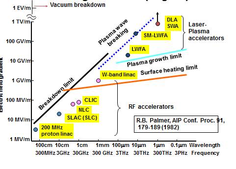
Fig. 1: Gradients of accelerating field vs. the operation frequency.
These accelerating structures are integrated in a single device, a standing wave (SW) structure and a traveling wave (TW) structure. The first part of the injector which house the photocathode works in the SW regime as π mode, the second part which includes the coupler of the power supply of the entire structure operates in the TW regime with the 2π / 3 mode. Compared to conventional structures, the latter configuration is not only compact, but allows to obtain the same beam quality using lower field gradients, with obvious advantages in terms of efficiency, cost and reliability. These devices are simple, compact, efficient and certainly less expensive than conventional systems. They also allow producing particle beams of high brightness with peak currents between 50 and 200 A and emittance less than 2 mm-mrad. To further reduce the length of the electron bunch the device may operate as an integrated "velocity bunching" device. In this case the phase relationship between the accelerating fields of the SW and TW sections necessary to produce the compression of the bunch and, to increase the peak current, can be obtained by a suitable dimensioning of the length of the coupling cell.
The experimental characterization of RF hybrid structures however requires the development of methodologies different from those used for standard structures, especially those in the X-band. This is an additional source of interest for the accelerator physics community. The study and the realization of an accelerating X-band structure is a key issue for the evolution of photoinjectors. The interest for this type of project has been determined by both the feasibility of a hybrid X-band photoinjector, already demonstrated and, by dynamics simulations that confirm the possibility to produce high quality beams.
The availability of ultrashort bunches with high peak current makes possible the generation of monochromatic X-rays (narrow-band) sources from the Compton back-scattering with a large number of possible applications: medical (diagnostic mammography with photons in the 15-25 keV energy range, angiography of ~30 keV photons, computed tomography with photons in the 30-45 keV range), materials science (absorption and scattering of photons in the 3-30 keV range), biophysical (diffraction protein crystals, absorption, scattering at low angle with photons in the 10-20 keV range), etc..
The LNF have also realized high gradient accelerating structures at 11,424 GHz with results at high power comparable to those of structures made at SLAC and KEK with different technologies. Test performed at high power in the X-band at SLAC and KEK show the presence of electrical discharges particularly in the proximity of the irises, resulting in a perforation of the associated inner surfaces and the concomitant damage of the geometry of the coupling windows due to the heating "stress", with an additional impedance mismatch between power supply and accelerating section. Despite these effects, the accelerating structures of 'hard' type offer best experimental results in terms of accelerating gradients compared to traditional structures, according to standard brazing methods at high temperature. The performance of accelerating structures operating at 11,424 GHz of TW type has a behavior in terms of the accelerating gradient, 40% worse than that of the SW (soft) structures using the same materials, e.g., OFHC copper. This contradiction is not understood and this is just one reason to continue the R&D of innovative materials and technologies, the only route to improve performances of these structures.
Recently we also started a R&D activity on brazing, electroforming and Electron Beam Welding (EBW) procedures for the construction of structures of hard type with OFHC Cu and Cu-Zr. Are also under study, materials different from copper such as molybdenum (characterized by a higher melting point than Cu alloys) in order to increase, especially for X-band structures, the accelerating electric fields, while reducing the discharge phenomena which induce an irreversible damage to these structures.
Another field in which the R&D activity has just started in collaboration with LNL and CNR concerns the possibility to reduce the effects of pulse heating and electrical breakdown through the surface treatment of the copper cavities by deposition of suitable micrometer layers of molybdenum, ruthenium or other high temperature metals whose microstructure, thermal behavior and chemistry is compatible with the long term operation of the accelerating structures and their fabrication methods.
This is a very innovative approach to obtain surface engineered.??? Assuming that the interested region is concentrated in the outermost few micron from surface (compatible with the skin depth of GHz EM radiation), the idea is to hinder the deleterious effects of pulse heating (change of microstructure, modification of surface texture and development of inter-grain defects) through the deposition of fully dense, nano-structured coatings with given nano-structure (typically fine nano-crystals nano-composited or amorphous, or multilayer with nanometer periodicity). Metal multilayer may be deposited onto the surface to guarantee long term stability of accelerating structures. In addition to this also electrically insulating buffer layers may be deposited, to test EM surface and sub-surface effects.? The R&D on new coating materials needs to be developed both in the direction of testing new advanced layer configurations and innovative deposition techniques to be applied to fabrication by electroforming and to other complex 3D structures. This entails the need to set-up novel deposition methods based on bias sputtering and ionized sputtering that preserve tight work-piece tolerances (of order of 1-2 micron) and low roughness? (20-50 nm or better).
The main objectives of the above accelerator R&D activity are:
1) Construction of SW structures composed of three cells, with a central cell with an electric field twice that of the side cells;
2) Construction of three-cell SW structures to study independently the effect of discharges due to thermal 'stress' or to the 'pulse heating" in comparison with that associated to the electric field on the iris or in the vicinity of the same;
3) Alternative technologies to achieve a high surface quality (<20 nm);
4) Use of materials with a high melting point such as molybdenum and ruthenium? (e.g., Mo, Ru sputtering on copper).
5) Deposition of engineered multilayers of metals and metal-loaded-carbides and electrically insulating layers by advanced ionized/bias sputtering methods on flat (3”) samples and onto complex 3D geometries.
6) Characterization with Ion Beam Analysis (IBA) using LNL interdisciplinary accelerators, including proton microprobe analysis, of all produced layer composition, depth profile, thickness, density, conformal coverage analysis.
7) Characterization of smart coatings through morphological (AFM, SEM, FIB, etc.) and structural techniques (XAS) will be accompanied by standard electric and mechanical tests of 3" samples with coatings of metals and carbon-based nano-materials (nano-tubes, graphene and specific metals (Mo, CuZr etc. etc) obtained by sputtering and electro-spray deposition after surface treatment procedures for removal of oxide insulating layer and for optimized adhesions. The 3" samples will be placed in "rf pulse heating" accelerating cavities for direct comparison with oxygen-free high conductivity (OFHC) copper. In particular the role of exceptional thermal and electric conductivity of nano-carbon materials will be used, by using sputtering UHV techniques, and directly from a liquid phase, paying attention to the best method to reduce the contact resistance at the grain boundaries of the material forming the thin film, as measured by ex-situ characterization by AFM and four probes electric measurements. To find the best condition of operation the samples will be also tested by mechanical, thermal and electric stress in situ during preparation of the coating to investigate in real time the spectroscopic and structural properties of the metal/metal and metal/carbon interface.
In this context, the R&D activities of this proposal aims at the realization of novel RF accelerating structures of SW type at 11,424 GHz in order to:
1) promote within the INFN, the acquisition of innovative technologies based on new materials for the irises and the coupling windows, raising the threshold for the electric discharge;
2) identify spin-off for compact industrial-grade devices.
3) develop alternatives to normal linear colliders based on superconductive technologies;
4) manufacture structures relatively simple and compact for the production of high brightness electron beams for linear accelerators such as SPARC.
The work program may be divided schematically:
->Structural design of accelerating hard section operational at 11,424 GHz with an innovative technology and experimental characterization tuning a bi-directional approach;
->Experiments on test cavities to determine the best electroforming methodology using different materials;
->Building (2-3) prototypes consisting of three cells and their characterization at room temperature including the 'dual cavity'
->Construction and characterization by Ion Beam Methods and morphological techniques (AFM, SEM, FIB, etc..), micro-structural (XAS) and macroscopic (electrical conductivity, hardness, grain distribution, etc..) of samples (discs of 3") with coatings obtained with different techniques and different materials (e.g., Mo, Ru, carbon nanotubes, etc..) for "rf pulse heating" experiments with dedicated cavities for these tests.
(Back/Home)
|